Stop Missing Wafer Defects: Reliable Semiconductor Microscopy Tools
By Omar Haddad • 29th Nov
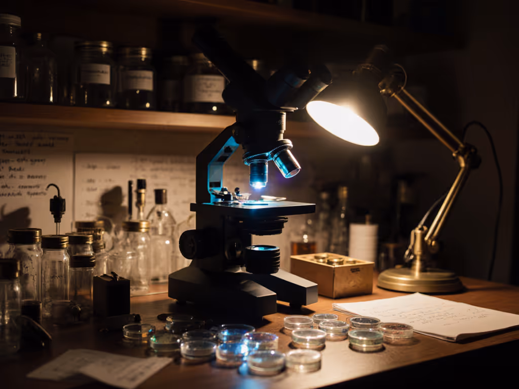
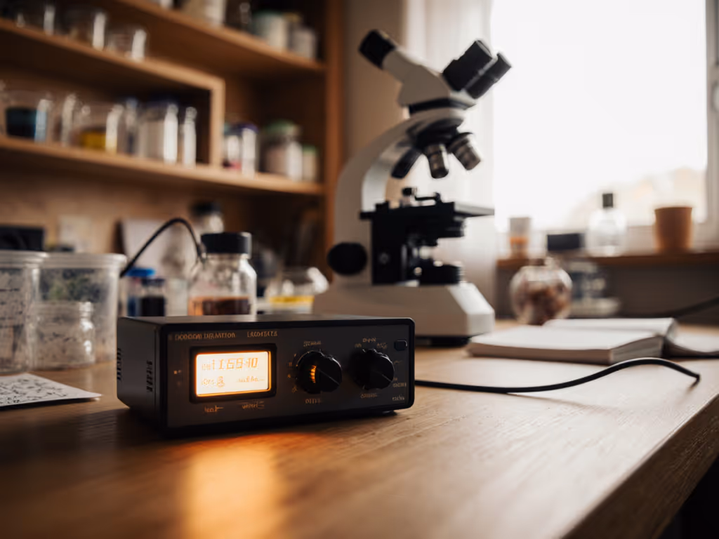
If you've ever held a discarded computer chip up to a window and wondered what microscopic worlds hide inside, semiconductor microscopy might be your new favorite adventure. Wafer inspection isn't just for billion-dollar factories, it's a thrilling entry point for hobbyists to explore the invisible architecture powering our digital lives. Forget intimidating jargon or lab coats; with the right affordable tools, you can uncover hidden patterns in silicon wafers from old electronics and feel that electric aha! moment when you spot your first tiny defect. I've seen this spark ignite countless times, like when a nine-year-old in my workshop found tardigrades using only a $2 pipette and a plastic slide. Small wins today grow into tomorrow's confident discoveries, and the same applies to understanding chips. Curiosity scales with confidence, especially when you start with tools that forgive mistakes and celebrate progress.
Why Wafer Inspection Isn't Just for Big Labs (It's for You!)
You might think wafer inspection belongs in sterile cleanrooms with million-dollar machines. But here's the truth: every smartphone you've recycled, every old circuit board from a thrift store, contains a silicon wafer waiting to be explored. Hobbyists like us are uniquely positioned to appreciate this up close (without the pressure of industrial yields). When I first started, I salvaged wafers from broken calculators and used my basic microscope to hunt for flaws. It felt like detective work, and honestly? It is. Spotting scratches, dust particles, or etching errors (defect detection made personal) turns abstract "semiconductor science" into tangible, rewarding puzzles.
Yet many beginners hit walls immediately:
- "My microscope shows blurry streaks, not crisp circuit lines" -> Missing proper lighting and prep
- "Professional tools cost more than my car!" -> Overlooking hobbyist-friendly alternatives
- "I found a weird spot - is it a defect or just a scratch?" -> Lacking context for IC analysis
These frustrations mirror what I hear in online forums: eagerness curbed by unclear guidance. To fix glare and those 'blurry streaks,' start with our guide to condenser light control. But what if I told you the gear you actually need fits in a shoebox? Let's rebuild this from the ground up, safely, affordably, and joyfully.
Your Starter Kit for Meaningful Wafer Exploration
Forget "all-or-nothing" thinking. Reliable semiconductor microscopy starts with scaffolded steps that build competence without overwhelm. I've curated tools that prioritize forgiving setup and clear learning curves, because when you're not wrestling with clunky gear, wonder takes over. Here's what works for beginners (tested with real hobbyists!)
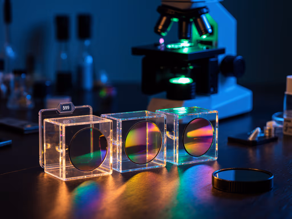
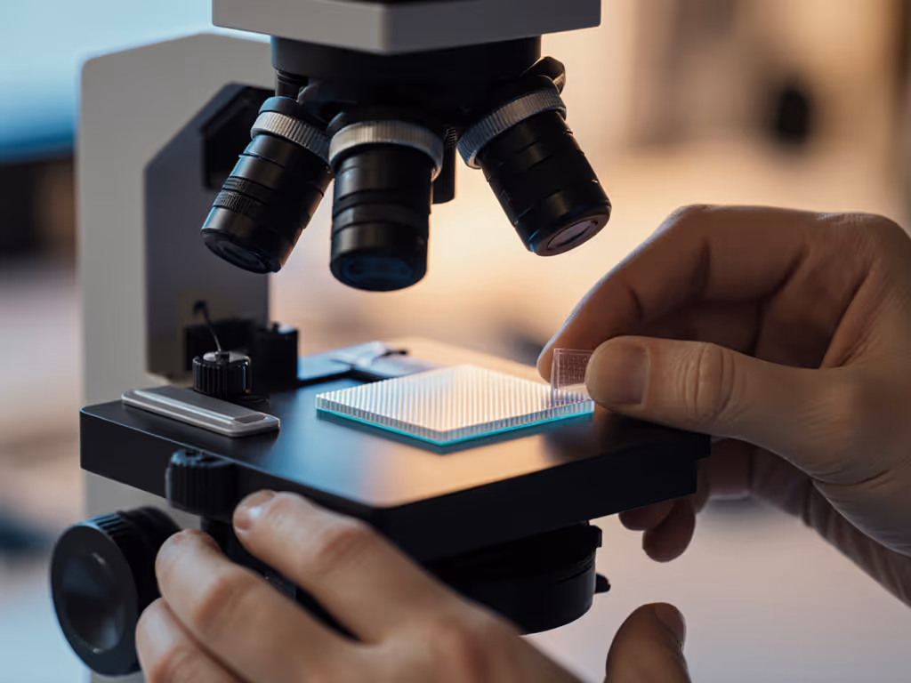
1. The Brightfield/Darkfield Adapter: See Defects Without the Drama
Most hobbyist microscopes default to brightfield lighting, fine for leaves or pond water, but awful for shiny silicon wafers. Light reflects everywhere, drowning out subtle scratches or particles. Enter the dual-mode adapter: a $30-$50 attachment that flips between brightfield (for general viewing) and darkfield (for defect hunting). In darkfield mode, light strikes the wafer at an angle, making defects glow against a dark background. Suddenly, those frustrating "blurry streaks" become visible pits or dust bunnies! When you're ready to quantify what you see, use our microscope measurement tools to size defects correctly.
I watched a retiree named Maria gasp when she first spotted a hairline crack in a wafer from her old GPS unit. "It's like finding dinosaur bones in my backyard!" she texted me later. That's the magic, defect detection that feels like treasure hunting.
Why hobbyists love it:
- No rewiring or calibration, just clip it onto your existing scope
- Reveals defects invisible under standard lighting (like shallow trench isolation voids)
- Perfect for precision metrology on a budget; measures flaw sizes via smartphone apps
My gentle nudge: Start with unpatterned wafers (like blank silicon test chips from eBay). Patterned wafers (with actual circuits) are dazzling but overwhelming. Build your "defect eye" slowly!
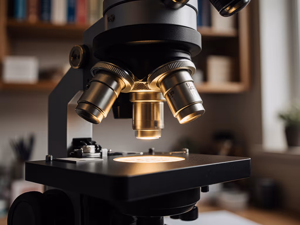
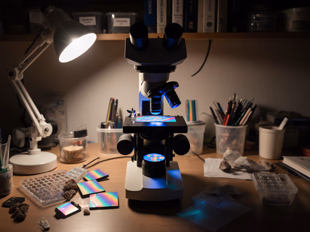
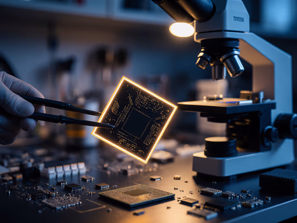
2. The USB 4K Microscope: Your Pocket-Sized Semiconductor Lab
Want IC analysis without liquid nitrogen or cleanrooms? USB microscopes (like the OptiScope Pro) plug into laptops or tablets, turning any surface into a wafer inspection station. Their magic? Integrated LED rings and computer-assisted focus. At 400x magnification, you'll see bond wires, solder bumps, and even transistor arrays. But the real game-changer is defect mapping: software highlights anomalies by comparing adjacent chip areas (mimicking industrial differential image detection) but simplified for beginners. For a deeper look at acquisition, analysis, and sharing, explore microscopy workflow software.
Key perks for solo explorers:
- Saves images/videos instantly for sharing in hobbyist communities
- Measures defect sizes accurately (no eyepiece graticules needed!)
- Works flawlessly with flat samples like wafers (no slide prep required)
My gentle nudge: Practice on decapped chips first (search "chip decap tutorial"). Seeing the raw silicon die builds context before tackling intact wafers. And yes, those rainbow swirls you'll spot? Often just oxide layers, not defects! Context is everything.
3. The Precision Stage Add-On: Stop Hunting, Start Finding
Nothing kills joy faster than losing your place on a wafer. Industrial inspectors use motorized stages, but hobbyists can achieve similar results with a $60 manual X-Y stage. If you're weighing mechanical versus motorized upgrades, see our microscope stage types overview. This slide-holder glides smoothly under your microscope, letting you grid-search wafers methodically. I call it the "beginner's defect detector": map coordinates, revisit spots, and build confidence through repeatable discovery.
Why it's non-negotiable for serious hobbyists:
- Turns random wafer scanning into structured wafer inspection
- Enables collaborative "defect hunts" (e.g., "Check sector C-7 next!")
- Compatible with all upright microscopes (no model fuss)
Pro tip: Use free apps like WaferMapper to log defect locations. Over time, you'll spot patterns (like how edge defects cluster near wafer handles).
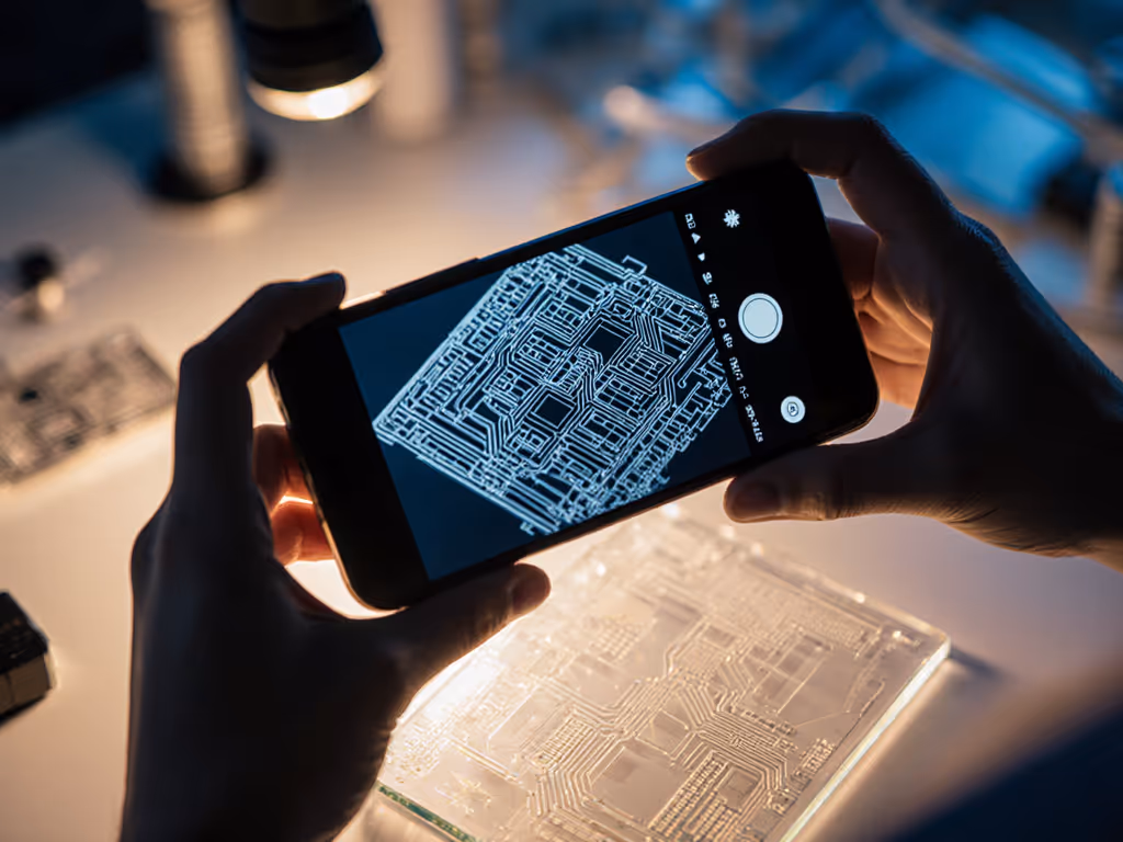
4. Smartphone Photomask Viewer: Decode the Invisible Blueprints
Photomask inspection sounds impossibly technical, until you realize photomasks are just stencils for etching circuits. And guess what? You can examine them using your phone! The Photomask Lens Kit (a clip-on macro lens + diffuser) turns your smartphone into a low-mag inspection tool. Shine a flashlight through a salvaged photomask (eBay has them!), and you'll see the circuit blueprint clearly. It's IC analysis made tactile and immediate.
Why beginners adore this:
- Zero microscope required, perfect for testing interest
- Builds intuition for how wafers are made (not just inspected)
- Makes abstract concepts like "lithography" feel real
My gentle nudge: Start with simple LED flashlights. Laser pointers cause glare, frustration awaits! Remember: accessible tools turn curiosity into repeatable discovery.
Building Your Workflow: From Frustration to First Discoveries
I've guided hundreds into wafer microscopy, and the winners follow this golden rule: Start stupidly simple. Don't mimic factory protocols; build your own rhythm. Here's my recommended starter routine:
- Salvage safely: Extract wafers from non-battery electronics (e.g., old calculators). Never use power tools near silicon, sharp fragments fly!
- Clean gently: Wipe wafers with 99% isopropyl alcohol and a lint-free cloth (coffee filters work!). Water leaves spots. For optics that stay crisp and dust-free, follow our microscope maintenance guide.
- Inspect in stages:
- First pass: Brightfield mode to spot big debris
- Second pass: Darkfield mode for subtle defects
- Third pass: Precision stage for mapping
- Document everything: Note wafer source, lighting, and defects. Patterns emerge over time!
"Wait, why not just buy a fancy microscope?" Because your current scope can do this. My $200 entry-level scope found tardigrades, then wafer defects. Upgrading tools after you've mastered basics beats drowning in complexity. Curiosity scales with confidence.
Your Journey Starts with One Defect
You don't need plasma illumination or atomic force probes to begin. Industrial wafer inspection tools chase nanometer-scale flaws for billions in yield, your goal is wonder, not wafer lots. And that's beautiful. Every scratch you spot, every bond wire you trace, connects you to the engineers who built our digital world. It's mindfulness with a microscope, where patience reveals universes in silicon.
I'll leave you with this: Last week, a hobbyist emailed me blurry photos of a chip defect he'd found. "It's probably nothing," he wrote. But it was something, a rare etching error! Now he's documenting defects for a YouTube channel. His tools? The brightfield/darkfield adapter and USB scope featured here. That's the power of starting small.
Ready to see what's hiding in plain sight? Dive deeper with these free resources:
- 半导体微观探索 (Free wafer defect ID guide for beginners)
- 社区论坛链接 (Join 2,000+ hobbyists sharing DIY inspection tips)
- 视频教程链接 ("Wafer Inspection in 20 Minutes" - no jargon, promise!)
Your next discovery is waiting. All it takes is a curious eye and tools that grow with you. Because when wonder becomes repeatable? That's when science truly begins.
Related Articles